
SAN JOSE, Calif., Feb. 26, 2019 /PRNewswire/ -- The eBeam Initiative, a forum dedicated to the education and promotion of new semiconductor manufacturing approaches based on electron beam (eBeam) technologies, today announced that ASML Holding N.V. (ASML) has joined the eBeam Initiative. As one of the world's leading manufacturers of chip-making equipment, ASML will provide its valuable perspective to the educational activities of the eBeam Initiative within the semiconductor photomask and lithography supply chain.

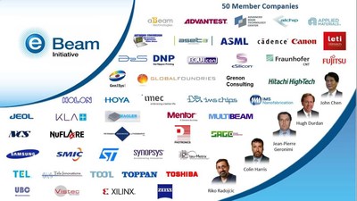
In 2009, the eBeam Initiative was launched to provide a strong voice and educational platform for eBeam technology within the photomask and semiconductor design and manufacturing community. Instrumental to its efforts, the eBeam Initiative leverages its annual perceptions and mask maker surveys to confirm key trends to help guide the industry forward in supporting the introduction of new eBeam technologies. In achieving a new milestone with 50 member companies, the eBeam Initiative continues its charter to enable industry collaboration to advance the eBeam technology ecosystem.
Today, during the SPIE Advanced Lithography Conference being held at the San Jose Convention Center, the eBeam Initiative will host its annual luncheon event featuring presentations from Dr. Yu Cao, senior vice president of ASML; Dr. Harry Levinson, principal at HJL Lithography; and Dr. Leo Pang, chief product officer and executive vice president at D2S. These industry luminaries will cover several eBeam-related topics key to the future success of photomask manufacturing and lithography, including: computations for EUV lithography; GPU-accelerated simulation enabling applied deep learning for photomasks; and applications of machine learning in computational lithography. Copies of these presentations will be made available after February 26 on the eBeam Initiative website at www.ebeam.org.
"ASML will provide valuable perspectives to the eBeam Initiative," stated Aki Fujimura, CEO of D2S, managing company sponsor of the eBeam Initiative. "ASML has significant expertise in modeling and simulation of the lithography process as well as eBeam metrology and inspection, the latter through the acquisition of HMI. This offers expanded insights for eBeam mask writing around metrology and inspection, as well as computational lithography. To continue to develop new innovations in eBeam technology, the need for collaborative industry efforts like those of the eBeam Initiative have never been more important. We are very pleased to welcome ASML as our newest contributor to our mission to provide industry collaboration for new semiconductor manufacturing approaches that accelerate the use of eBeam technology."
About The eBeam Initiative
The eBeam Initiative provides a forum for educational and promotional activities regarding new semiconductor manufacturing approaches based on electron beam (eBeam) technologies. The goals of the Initiative are to reduce the barriers to adoption to enable more integrated circuit (IC) design starts and faster time-to-market while increasing the investment in eBeam technologies throughout the semiconductor ecosystem. Members, which span the semiconductor ecosystem, include: aBeam Technologies; Advantest; Alchip Technologies; AMTC; Applied Materials; Artwork Conversion; Aselta Nanographics; ASML; Cadence Design Systems; Canon; CEA-Leti; D2S; Dai Nippon Printing; EQUIcon Software GmbH Jena; eSilicon Corporation; Fraunhofer CNT; Fujitsu Semiconductor Limited; GenISys GmbH; GLOBALFOUNDRIES; Grenon Consulting; Hitachi High-Technologies; HOLON CO., LTD; HOYA Corporation; imec; IMS CHIPS; IMS Nanofabrication AG; JEOL; KLA; Maglen; Mentor, a Siemens Business; Multibeam Corporation; NCS; NuFlare Technology; Petersen Advanced Lithography; Photronics; Sage Design Automation; Samsung Electronics; Semiconductor Manufacturing International (Shanghai) Corporation (SMIC); STMicroelectronics; Synopsys; tau-Metrix; Tela Innovations; Tokyo Electron Ltd. (TEL); TOOL Corporation; Toppan Printing; Toshiba; UBC Microelectronics; Vistec Electron Beam GmbH; Xilinx and ZEISS. Membership is open to all companies and institutions throughout the electronics industry. To find out more, please visit www.ebeam.org.
SOURCE eBeam Initiative
